
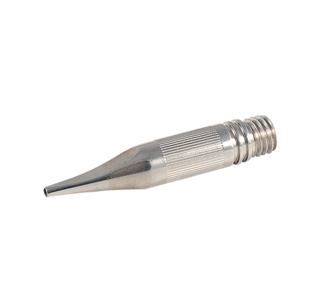
The metal soldering iron tip is specially designed for welding optical precision parts. It uses a high-purity oxygen-free copper alloy substrate, is precisely forged and nickel-plated on the surface, and presents a silver-white metallic luster. Its unique conical shape and the tip diameter are precisely controlled in a very small range, which is suitable for fine welding scenarios such as optical component pins and microcircuit solder joints. With a threaded interface, it can be firmly connected to professional welding equipment. In operations such as optical lens assembly, optical communication module welding, and microscope component repair, it can accurately transfer heat to achieve controllable melting and forming of solder, providing stable and high-precision tool support for the welding of optical precision parts, ensuring that the performance of the optical system is not affected by the welding process.
The nickel-plated surface hardness reaches HV200 or above, which is wear-resistant and not easy to get tinned, reducing the risk of solder residue contamination to optical parts; at the same time, it has good oxidation resistance. When used for a long time in a high-temperature welding environment, the surface of the soldering iron tip is not easy to oxidize and deform, ensuring stable welding accuracy.
Features | Parameters |
Advanced precision | Diameter tolerance ±0.01mm, suitable for solder joints below 0.3mm |
Temperature control performance | Heating to 350℃≤10s, small thermal diffusion range |
Surface characteristics | Nickel plating hardness HV200+, wear-resistant, anti-oxidation, low tinning |
3. Product Details
In the production process, 99.99% high-purity oxygen-free copper is selected, and the material density is improved through multiple forging processes. Then, the precise cone and thread interface are processed by CNC lathe, and finally the surface performance is enhanced by nickel plating.
The finished product is tested for tip accuracy by laser diameter gauge, and the temperature control and conduction performance is verified by thermocouple temperature measurement. In the assembly of optical lenses, the CCD sensor pins are welded to ensure the stability of imaging signals; in the production of optical communication modules, the optical fiber array and PCB board are precisely welded to ensure low-loss transmission of optical signals; when repairing microscopes, the circuit solder joints of the objective lens group are repaired to restore the clarity of optical observation. From research and development to application, with the characteristics of ultra-precision adaptation, precise temperature control, durability and anti-pollution, it has become a "precision scalpel" for welding optical precision parts, protecting the core performance of optical equipment.
 Headquarters tel.
 E-mail.
 China management center add.
204, Building A, Phase 3, Jiewei Industrial Park, Shangmugu Community, Pinghu Street, Longgang District, Shenzhen, China
 Headquarters tel.
+86 134 3077 5139
 E-mail.


 CN
CN


